Description
Wafer software: Raman/PL Analysis of Wafers Made Easy
Acquisition and Analysis functions dedicated to wafer geometry for a user-friendly, optimum efficiency experience. This App joins the LabSpec 6 Software Suite and ensures comprehensive exploration of parameters as a prerequisite for metrology deployment!
Compatibility:
This app requires the latest version of LabSpec 6. If you do not already own LabSpec 6, please go to the LabSpec 6 product page to purchase your LabSpec 6 license. If you already own LabSpec 6, you will be contacted by our service team for a free upgrade to the latest available version, if needed.
Conditions of use:
- App usable on a single PC
- Can be transferred to another PC via HORIBA
- Permanent license
- Free updates in LabSpec 6
Key Features:
- Precise stage positioning for loading sample and analysis
- Creation of acquisition and analysis templates
- Versatile sampling schemes
- Various autofocus modes
- Easy zoom‑area selection
- Real‑time analytics supported by multiple visualization
- Instant, customizable reporting
Details:
Wafer-level analysis is essential to monitor material uniformity, process stability, and device performance across manufacturing nodes. Early identification of spatial variability and defects enables faster process optimization and higher yield.
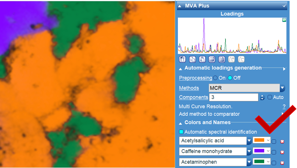
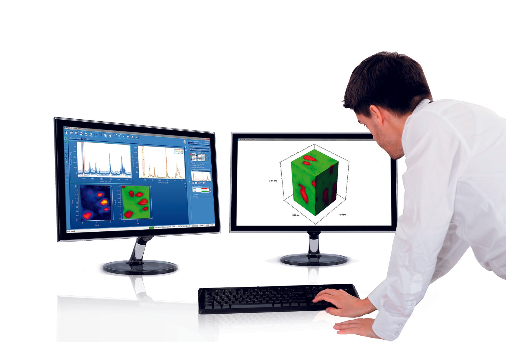
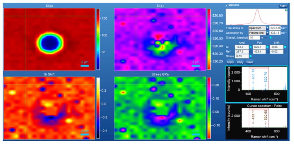
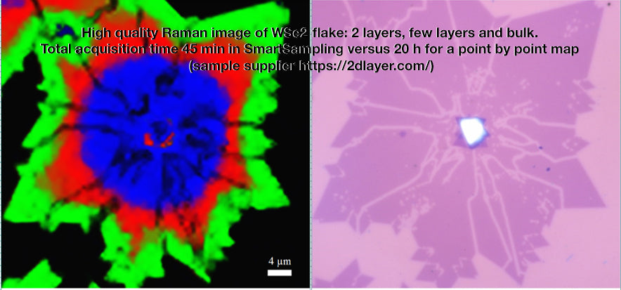
Raman and Photoluminescence (PL) spectroscopies are powerful, non-destructive techniques ideally suited for semiconductor wafer analysis, providing detailed insights into material composition, stress, and crystallinity. To fully leverage Raman/PL data at scale, dedicated analysis software is critical to efficiently extract meaningful information, ensure parameter space exploration, and support reliable metrology deployment.

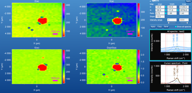
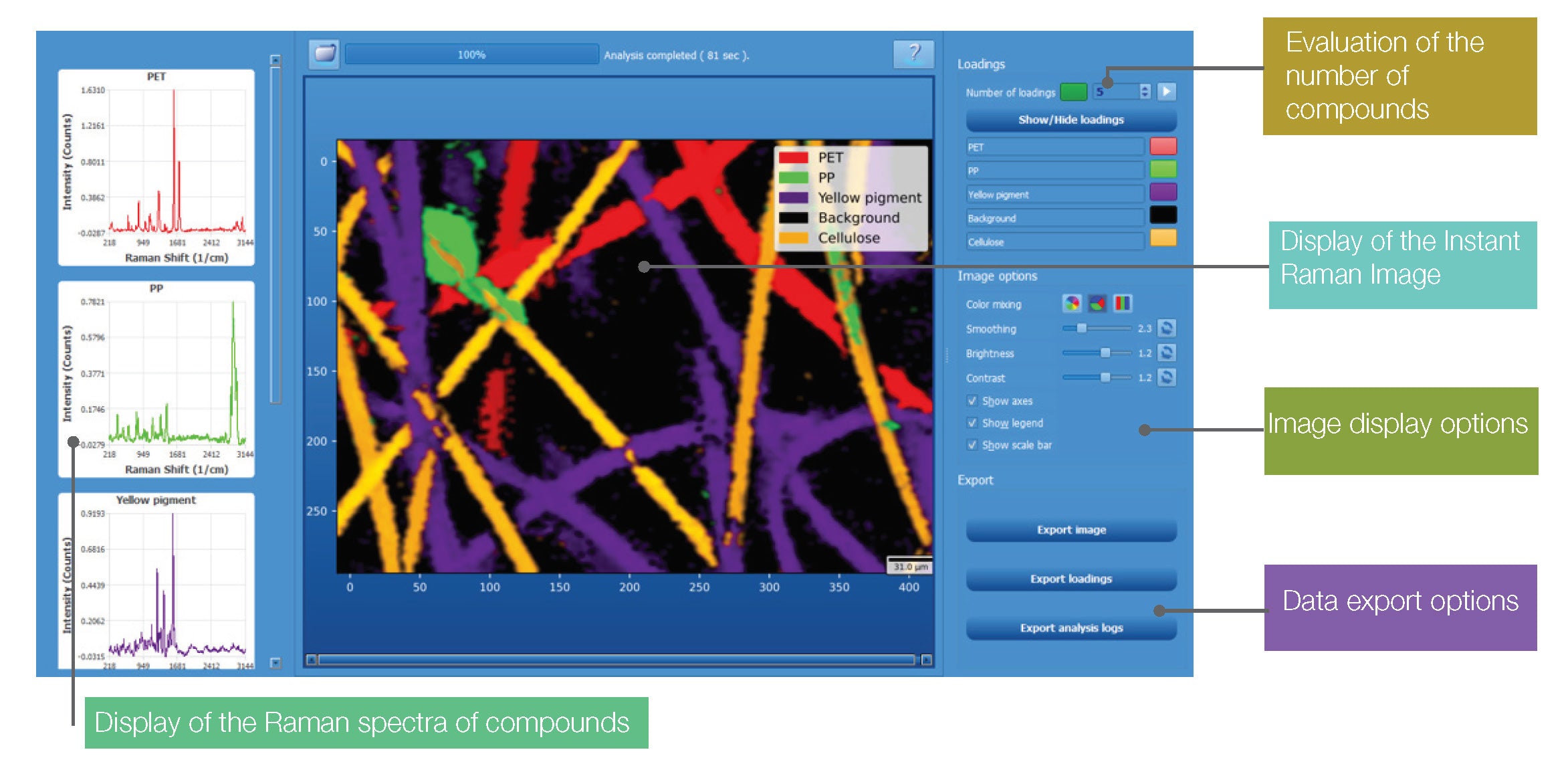
1. Sampling pattern
2. 2D width intensity map
3. I2D/IG width histogram
4. Selected point spectrum
5. Sample definition
6. Acquisition and analysis parameters
7. Statistical table
If you want more information about this topic, please visit our website on LabSpec 6 App for easy and ergonomic characterization of wafers
You may also like